
Introduction
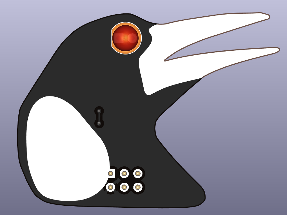
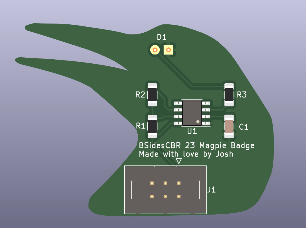
The goal of today’s workshop is to design and assemble a printed circuit board (PCB) which takes the form of a magpie with a blinking eye. Once assembled, the add-on will plug into your badge and scare everyone within swooping distance whilst reminding them that Birds Aren’t Real.
By the end of the workshop you’ll have learnt how to design a schematic and layout a PCB using KiCad, along with how to solder through hole and surface mount components.
Let’s Begin!
Before we dive into designing the PCB, we need to pick a CAD tool to use. Whilst there are online tools such as Easy EDA, they are limited in capability due to running in a browser and if you continue to design PCBs after this workshop may run into limitations. As such we will be using KiCad, an extremely powerful and open source EDA tool, which will handle whatever you can throw at it.
If you have not already installed KiCad, please download it from here. We will be using version 7 in this workshop, if you have an earlier version please update to V7 or proceed at your own peril!
You will also need to download the library I have made for this workshop, as it contains custom symbols and most importantly the artwork to make our badge look like a magpie.
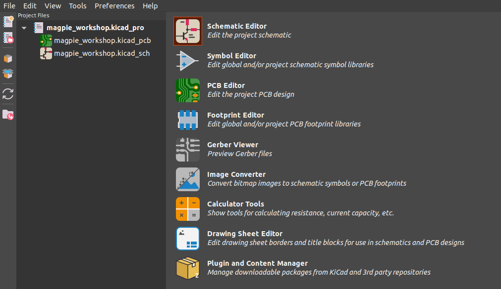
KiCad Project Setup
Prior to starting the design, we need to make a new KiCad project and add the above downloaded library so we can use the symbols and footprints.
- Open KiCad.
- File -> New Project.
- Give your project a fun name and a place to live.
- Extract the library files to within your newly created project folder.
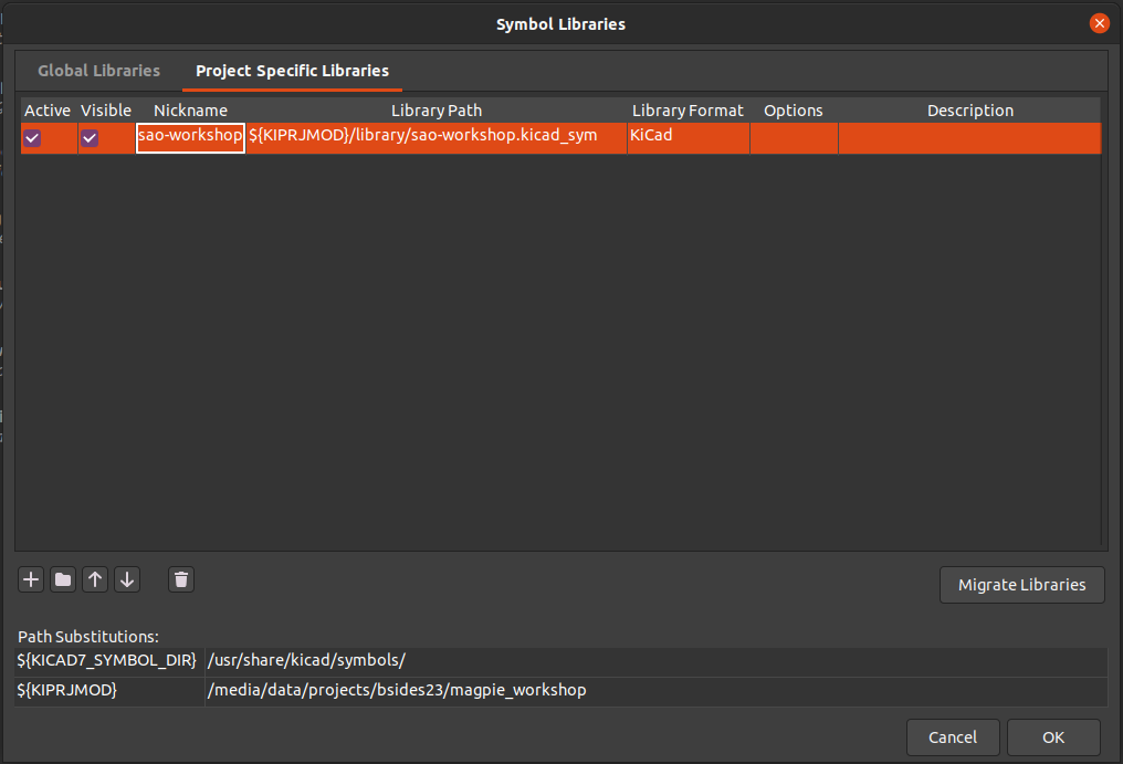
- Preferences -> Manage Symbol Libraries
- Change tab to “Project Specific Libraries”
- Click on the “folder” button, and select the
sao-workshop.kicad_symfile you downloaded earlier.
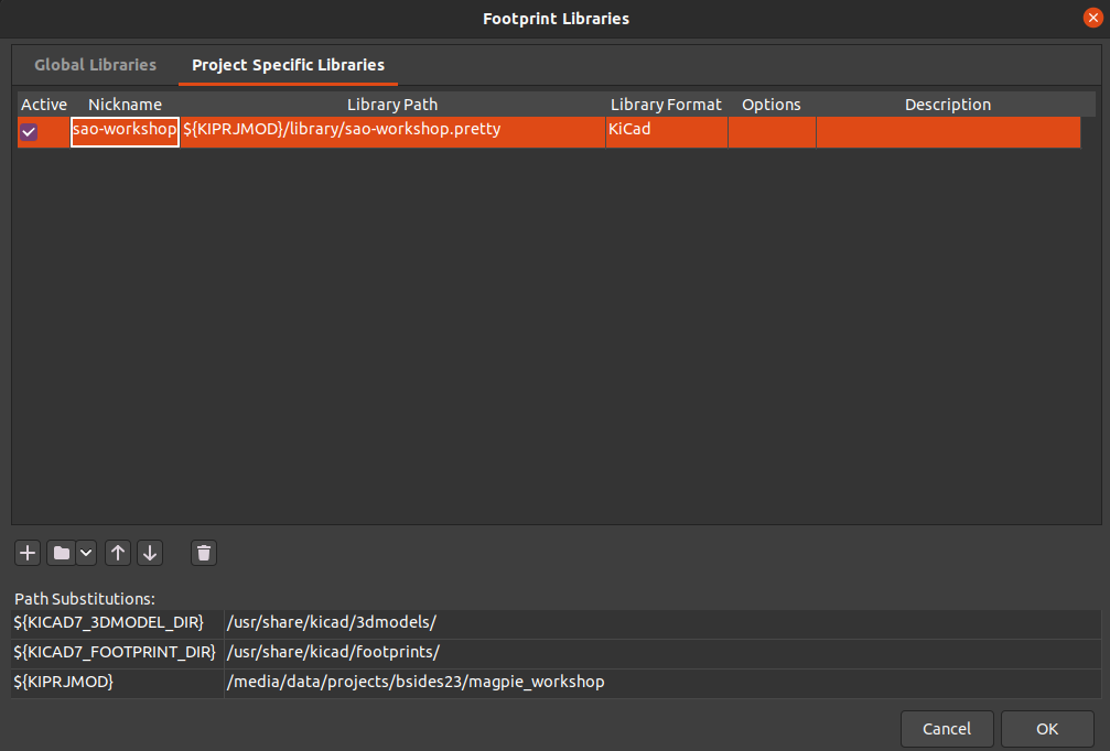
- Preferences -> Manage Footprint Libraries
- Change tab to “Project Specific Libraries”
- Click on the “folder” button, and select the
sao-workshop.prettyfolder you downloaded earlier.
With the project setup and libraries added, are now ready to draw up the schematic.
Schematic Capture
Schematic capture is the first step of the PCB design process, and involves drawing the circuit we want to design and defining what pins connect to each other. During this step we don’t have to follow the laws of physics which allows us to rearrange pins, use net labels to connect signals, and split the design across multiple sheets on a big design to draw the design in a way which is easy to read and understand.
KiCad Schematic Hotkeys Reference
| Shortcut | Function |
|---|---|
| A | Place (add) symbol |
| E | Edit symbol |
| M | Move symbol |
| R | Rotate symbol |
Functional Description
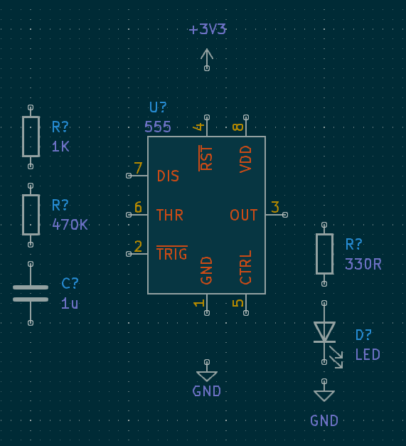
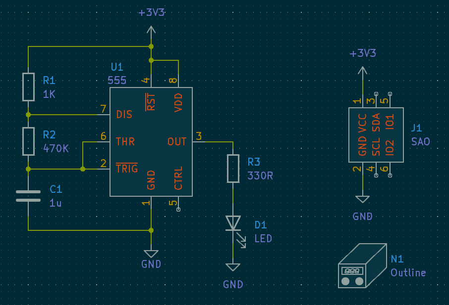
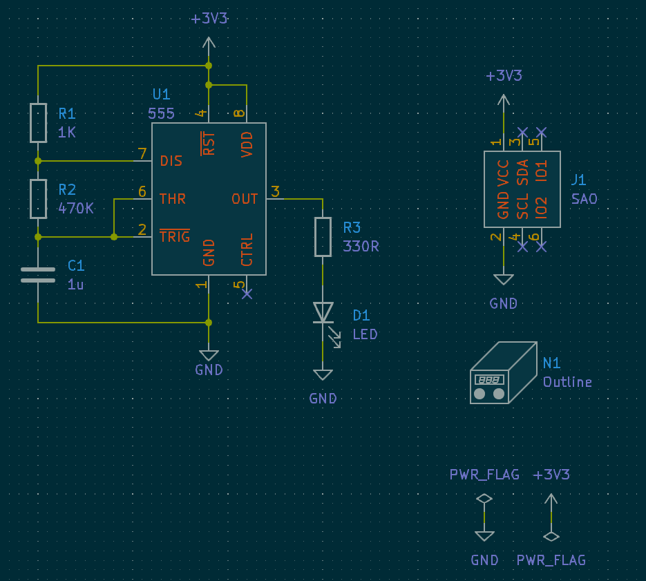
For this workshop we’ll be designing an astable 555 timer, which is a fancy way of toggling a pin (and in turn a LED) on and off forever. A simplified version of the circuit we will be designing is shown below.
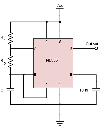
By varying the values of R1, R2, and C, we can adjust the frequency (how fast the output toggles from high to low) and the duty cycle (percentage of time the pin is high in a given period). The maths to determine the components values for a 50% duty cycle is below.
1
2
3
f = sqrt(2)/(C1(R1 + 2R2))
  = 1.4/(1u(1K + 2*470K))
  = 1.5 Hz
Drawing the Schematic
Open the schematic editor.
Press
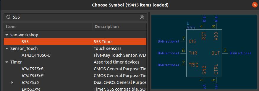
Ato add a new part, and select the 555 timer from thesao_workshoplibrary.
- Press
Aagain and add resistors (searchR), capacitor (searchC) and LED (searchLED) arrange as shown below. To rotate the symbol, pressRwhilst dragging the symbol.
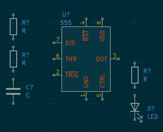
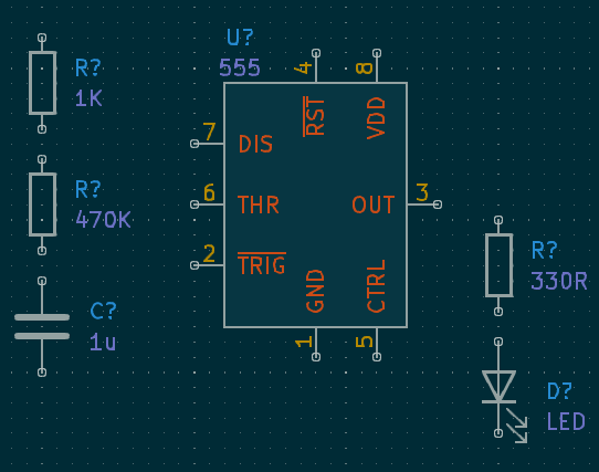
- Double click on each symbol and update the component values as shown below. The “K” stands for KiloOhms (1000 Ohms), and the ”u” for microfarads (0.000001 Farads).
- With the components placed, we can add the power and ground symbols by pressing
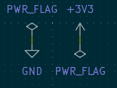
Athen searching for+3V3andGND.- “+3V3” and “GND” are magic symbols that put the badge voltage and ground anywhere on the board, and means you don’t have to run a wire to connect power/ground to every point on the schematic.
- Finally, with all these components placed, use the wire
Wtool to connect all the pins as shown below.
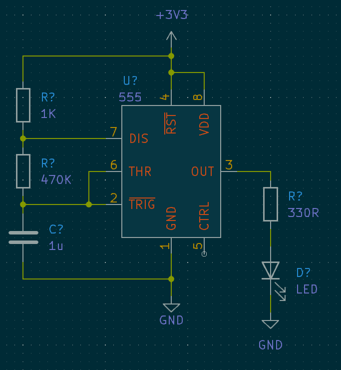
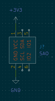
At this stage, we have the 555 timer all wired up, however we don’t have a way of supplying it with power. Your bPod has a SAO header on it which supplies the required 3V3 and GND connections, so let’s use that.
- Add the SAO connector by opening the choose symbol (
A) screen and searchingSAO. Then add +3V3 and GND symbols as shown below.
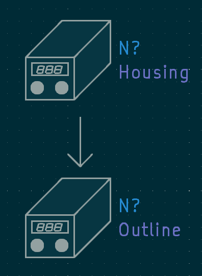
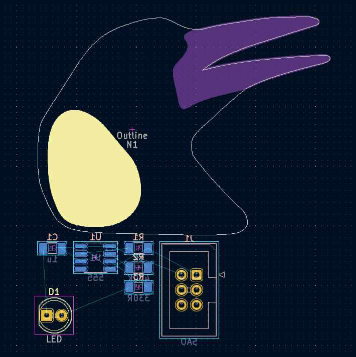
With this done, we’ve got all the electrical components required to blink a LED. However we don’t yet have the board in the shape of a magpie. As “magpie” isn’t a schematic symbol, we’ll add a dummy component which we will later assign to be the footprint of our magpie.
- Add a
Housingto the schematic and rename it toOutline.
This concludes placing parts in the schematic, and we can start setting things up for layout.
Annotation, Electrical Rules Check, Footprint Association
Currently our symbols are abstract objects that don’t have unique IDs or footprints associated to them, two things which are required to lay out the PCB.
- Annotate the schematic (assign unique numbers to each component) using the below button.
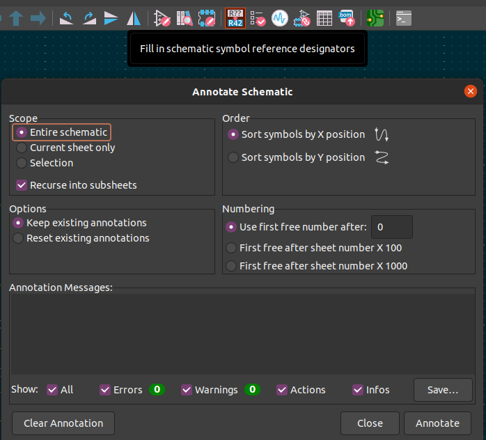
Once this is complete, you should have unique numbers on each component on the PCB.
We can now run Electrical Rules Check (ERC). ERC is a basic sanity check designed to find obvious issues such as pins which are not connected, two inputs connected to each other, or no power being provided to an IC, and it’s a good rule to not start PCB layout until your schematic is clear of ERC errors.
- Run ERC from the menu shown below, and you should get 8 errors.
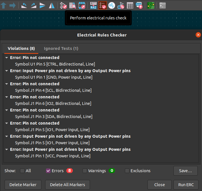
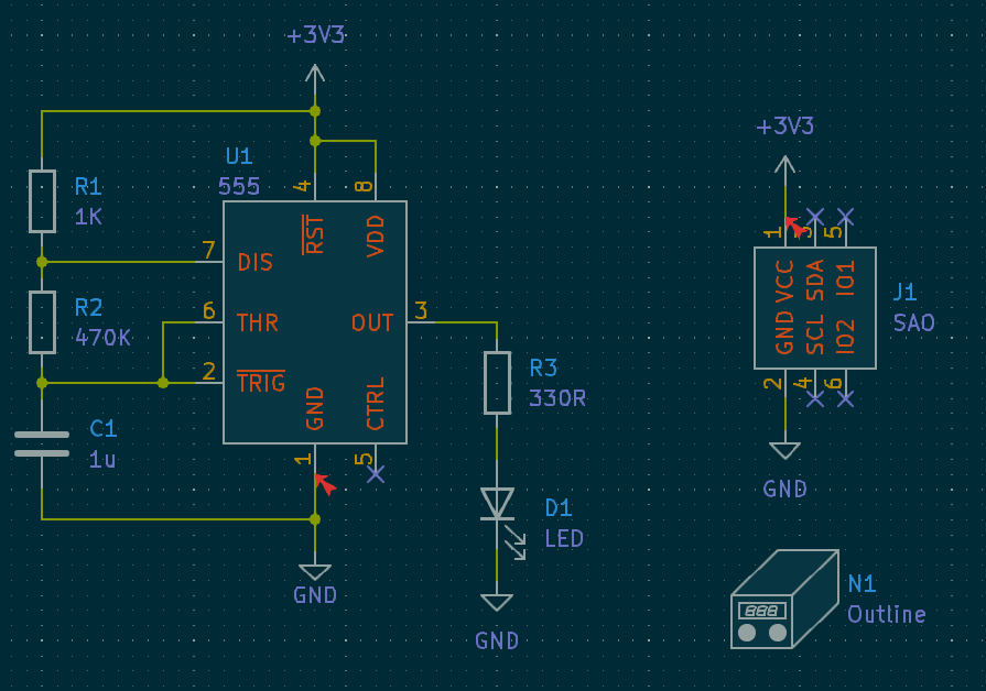
- Five of these errors are due to unconnected pins, and can be fixed by placing no-connection directives
Qon the unconnected pins to tell KiCad they’ve been left disconnected by design.
Run ERC again, and you’ll see two remaining errors for “Input Power pin not driven by any Output Power pins”. This is KiCad complaining because the 555 timer has power pins, but we haven’t told it the SAO header provides power, so it thinks the IC won’t get any power to turn on.
- This issue can be fixed by placing
PWR_FLAGon the 3V3 and GND nets to tell KiCad these nets are being driven by a power source.
With this last step, ERC shouldn’t have any errors (it’ll still have two warnings, but they’ll be ignored for this workshop), and we can continue to footprint association.
A given part (e.g. 1K resistor) can come in many different physical form factors, from large through hole power resistors, to tiny surface mount resistors found in modern electronics. To keep the number of components in the KiCad library down, they don’t make different symbols for each and every possible permutation, but instead get the designer to specify the footprint before moving onto PCB design.
- Using the footprint association tool, assign the correct footprints to the symbols as shown below. Note the
sao-workshop:magpie_outlinelibrary may be located at the bottom of the list, not in alphabetical order.
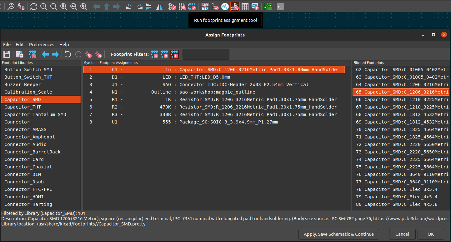
With the footprint association complete, we are ready to continue onto PCB layout!
PCB Layout
During schematic capture we told KiCad how we wanted to connect the components together. In layout, KiCad uses this information to assist us to make the connections whilst ensuring we follow the rules of physics this time. It’s like a big game of connect the dots!
KiCad PCB Hotkeys Reference
| Shortcut | Function |
|---|---|
| M | Move footprint |
| X | Route trace |
| V (whilst routing) | Place via |
| CTRL + SHIFT + V (not routing) | Place via |
| R | Rotate footprint |
| F | Flip footprint |
| H | Dim inactive layers |
| ALT + 3 | 3D Viewer |
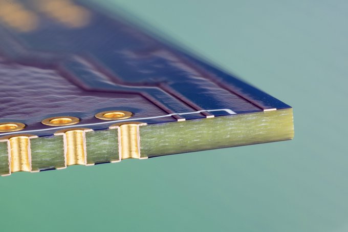
PCB Layers
A PCB consists of a number of layers of varying materials, and KiCad has a layer in the PCB layout tool that corresponds to each. The below are the ones we will be using in this workshop, and you can move between layers by clicking on it’s name in the PCB editor.
| Layer | KiCad | Colour | Function |
|---|---|---|---|
| Top Silkscreen | F.Silkscreen | Yellow | Markings on top of PCB |
| Top Soldermask | F.Mask | Purple | Negative outline of where copper should be exposed |
| Top Copper | F.Cu | Red | Copper on top of PCB |
| FR4 Core | N/A | N/A | Mechanical stiffness / holds PCB together |
| Bottom Copper | B.Cu | Blue | Copper on bottom of PCB |
| Bottom Soldermask | B.Mask | Green | Negative outline of where copper should be exposed |
| Bottom Silkscreen | B.Silkscreen | Peach | Markings on bottom of PCB |
| N/A | Edge.Cuts | White | Defines outline of PCB |
The below image from EMSL shows a cross section of a two layer PCB highlighting the above features, along with a cross section of a plated through hole.
Import Schematic
Before we can lay out the PCB, we need to import the schematic we defined in the earlier steps.
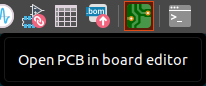
- Open the PCB editor (PCBNew).
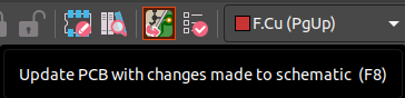
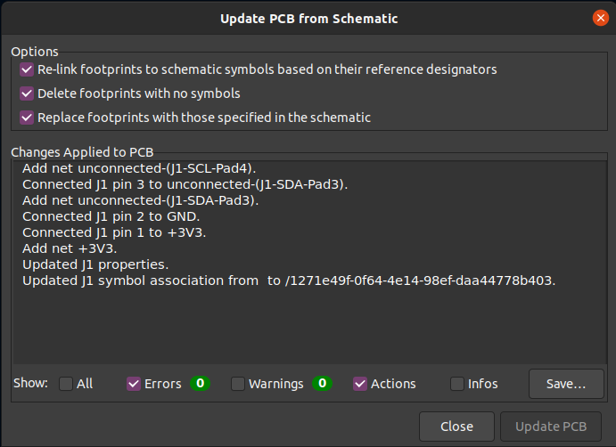
- Update PCB with changes from board editor.
- Select “Update PCB” and check that you don’t have any errors.
- You should now be able to left click and place all the components on the PCB.
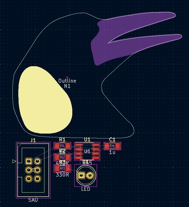
Placing Components
With the parts in the PCB editor, we need to place them on the PCB.
- This design will have all components other than the LED on the back of the board, so select them and press
Fto flip to the back. You’ll see their colour turn from red to blue.
We can now place the LED and connector in their locations, as they are fixed due to the mechanical design.
- First adjust the grid size to 0.1mm, as the 2.54mm KiCad ships with by default is too large.
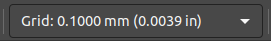
- Select the part, press
Mand move to the below locations. PressRwhilst moving to rotate.
- You can also look at the design in the 3D viewer
ALT + 3, as this can help determine if the mechanical parts are in the correct location.
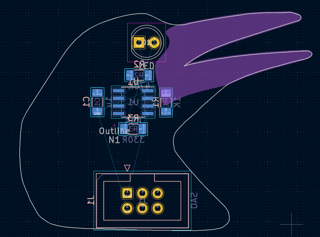
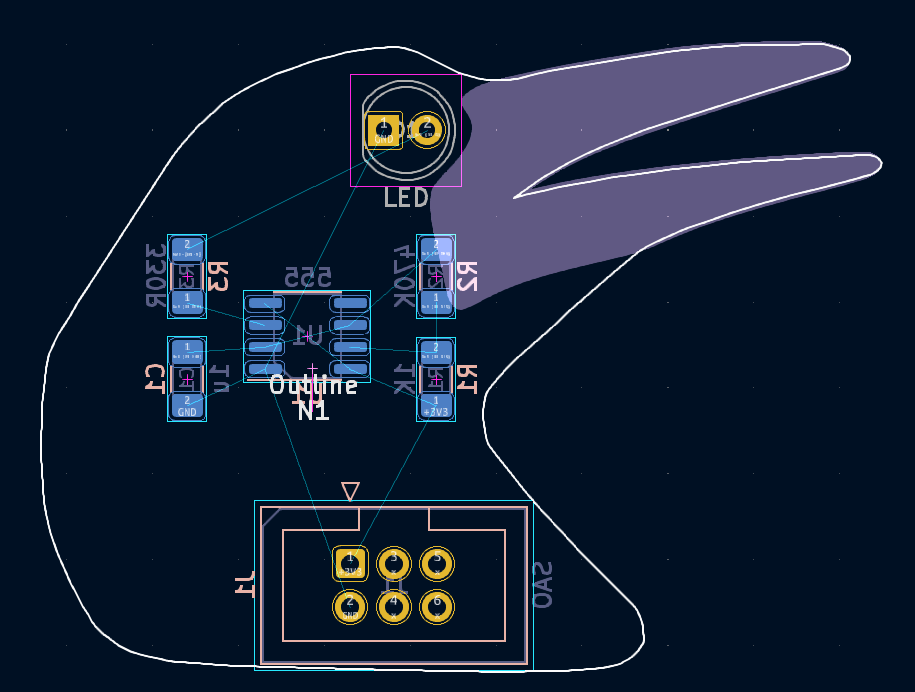
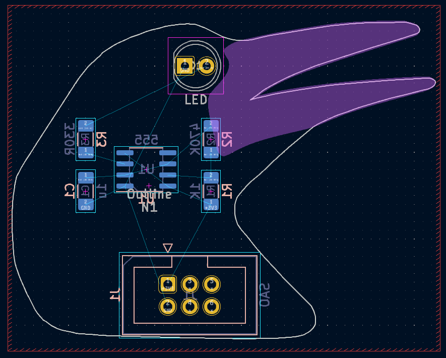
It’s now time to place all the electrical components on the PCB. Ideal component placement is a talk all in itself, but the primary goal is to have the fewest number of connection lines (typically called rats nests for some reason…) crossing as possible, as this will ease our routing step. I encourage you to try this step yourself before scrolling down to copy my solution.
- Select a part and press
Mto move it. - With the part selected, press
Rto rotate it. - Place the part on the PCB.
- Repeat for all other components.
- Keep going in an infinite loop until you are happy that there are as few connection lines as possible crossing.
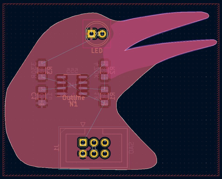
- You may want to turn off the F.Silkscreen (click the eye next to the name) so you can see the parts being placed on the PCB easier.
Poor component placement (lots of crossing lines).
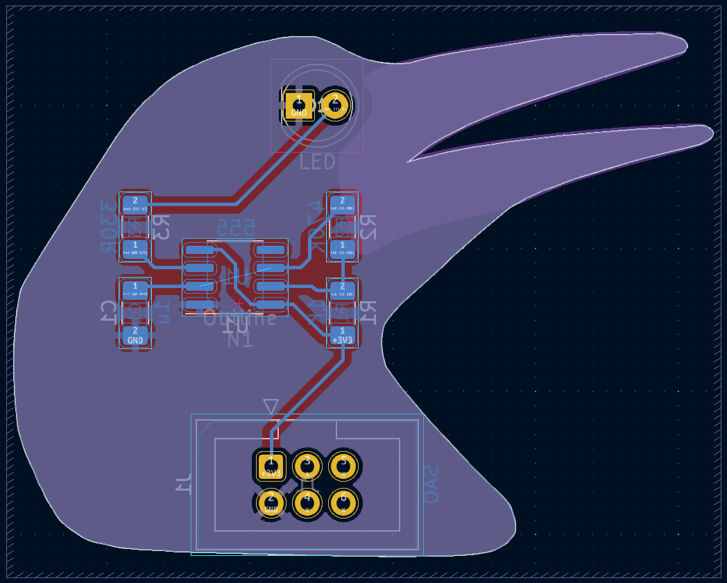
Good component placement (minimal crossing lines).
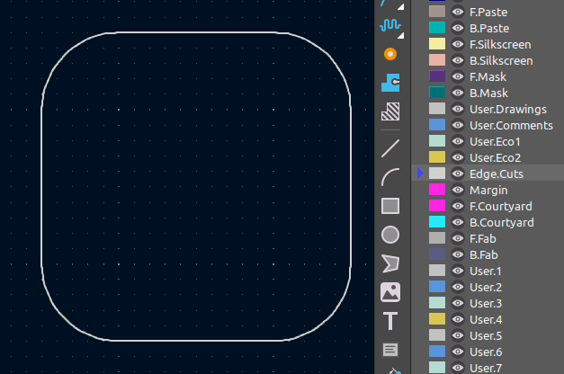
Defining Board Outline
Normally once you’ve placed the components on the PCB it’s time to define the board outline. However due to the magpie outline being provided this step isn’t needed today, but for future boards where the outline isn’t provided it can be done as below.
- Select the layer “Edge.Cuts”.
- Grab the line tool.
- Draw an enclosed shape.
- You can use the arc tool to give the PCB rounded corners.
Routing the PCB
Routing a PCB involves using copper to connect all of the required nets together so it functions correctly. Most PCBs will have a net called ground which most components connect to, so it’s common to dedicate an entire layer of the PCB to ground so make routing easier.
- Select F.Cu, click the “Add a filled zone” tool.
- Click anywhere on the PCB to open the menu.
- When you get to the popup screen, select both F.Cu and B.Cu, and net as GND.
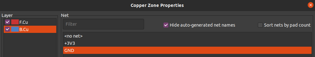
- Draw a box around the outside of the board, it does not need to follow the outline.
- Press
Bto fill all zones, and you’ll see the ground fills be poured and some of the connection lines go away as they are being connected by the plane.
It’s now time to route individual traces to get rid of the remaining connection lines.
- Hover cursor over a pad until it snaps.
- Press
Xto begin routing. - Move your cursor around to guide the trace, and left click to freeze the trace in place.
- Once you reach the other pad, wait for the cursor to snap to the pad and click to finish.
- Press
Bto repour the zone, which will move the pour away from the newly routed traces.
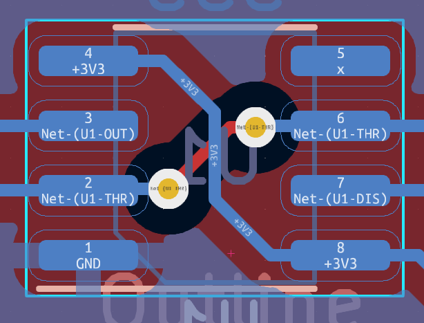
At this point you might find that it’s easy to route all but one of the traces. This is where we can use a via to change layers and make routing the impossible possible.
- Begin routing on the bottom layer as you were doing.
- Press
Vto drop a via and move to the top layer. - Move to the other side of the trace, and press
Vagain to place another via and return to the bottom copper. - Connect to the pad, and press
Bto repour the copper fill.
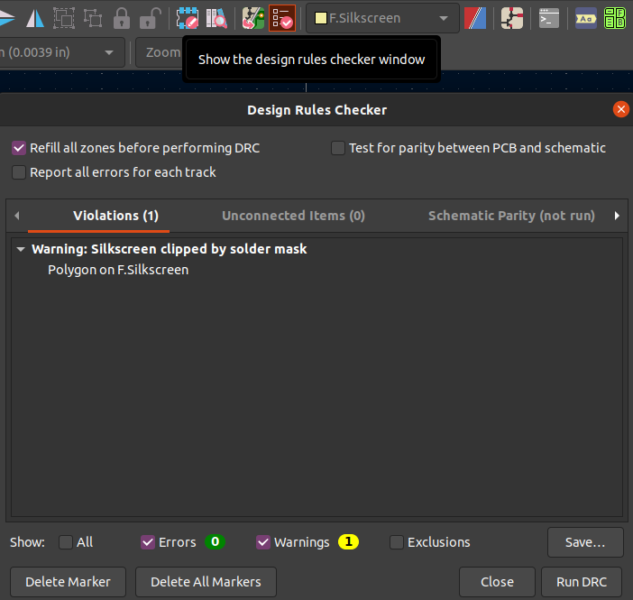
Design Rules Check
Whilst the PCB layout tool tries to prevent you from making mistakes, they always happen so it’s best practice to run Design Rule Checks (DRC) before ordering boards.
- Run DRC, and check there for errors. If there are errors, fix them and run DRC until they are all clear.
- Due to the artwork on the badge, it’s normal to get a warning about “Silkscreen clipped my solder mask” due to the location of the SAO connector.
Silkscreen
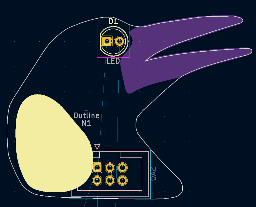
Now that DRC is clear, you are safe to order your PCBs knowing they’ll most likely work. However it’s also important for them to look nice, so let’s tidy up the silkscreen and add our name first.
- Press
ALT + 3to open the 3D viewer and look at the PCB. - You’ll notice D1 is on the front of the PCB, which is undesirable.
- Close the 3D viewer, select F.Silkscreen, click on D1, and press
Fto flip it to the back of the PCB.
- We can now add our name and any text you’d like on the back of the board by selecting B.Silkscreen, and using the text tool.
- We can now move the newly created text and any of the reference designators around using
MandRjust like we did with the components. - Use the 3D viewer
ALT + 3whilst doing this as it gives a much better idea of everything will look.
Exporting Gerbers and Ordering PCBs
Now that our PCB is complete, it’s time to generate the required files to order our boards!
- Using the Plot (not Print!) button, ensure all the layers we are using are selected, the plot format is Gerber, and plot the files to a folder of your choice.
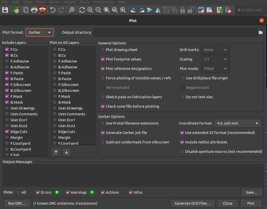
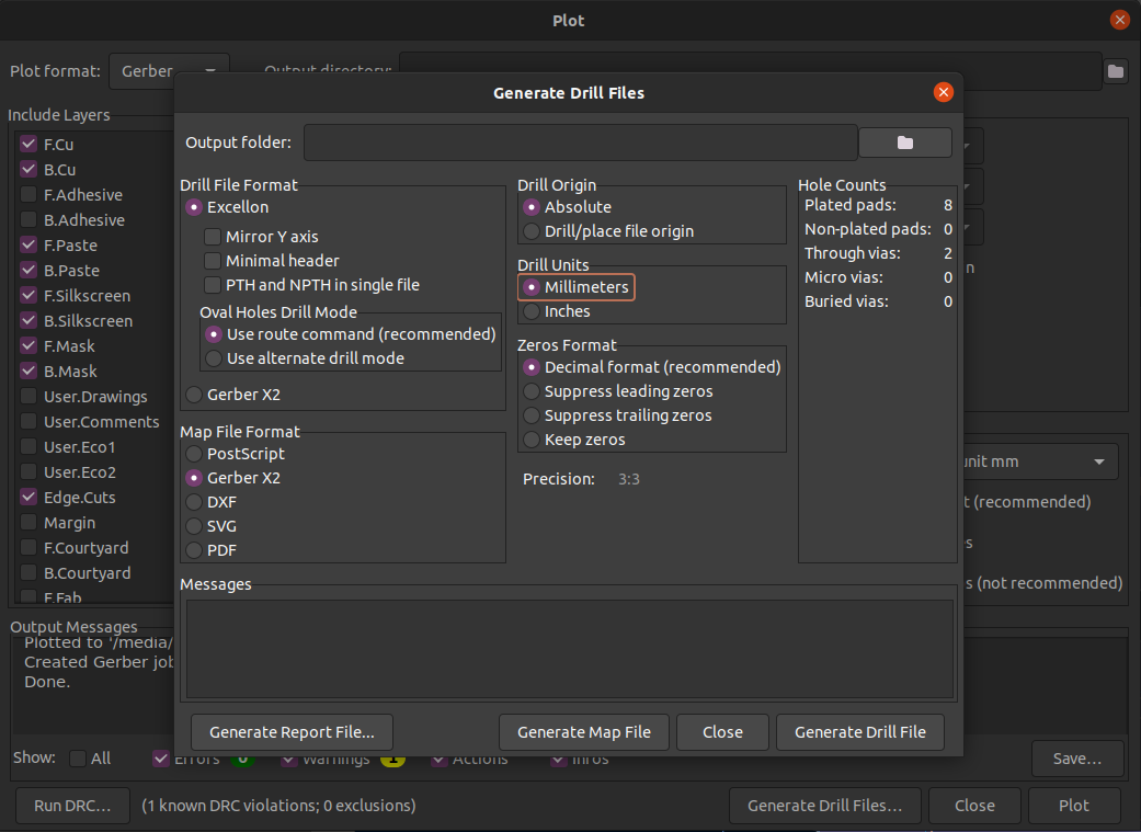
Keeping this window open, we also need to plot the drill files, as for historical reasons the gerbers do not contain the drill information.
- Select “Generate Drill Files”, check the settings are the same as the below image, and “Generate Drill File” to the same folder you picked before.
Before sending these files off, we’ll check them in KiCad’s inbuilt gerber viewer to check everything looks good.
- KiCad Homepage -> Gerber Viewer.
- “Open Autodetected files on new layer”.
- Select the gerbers and drill files exported earlier.
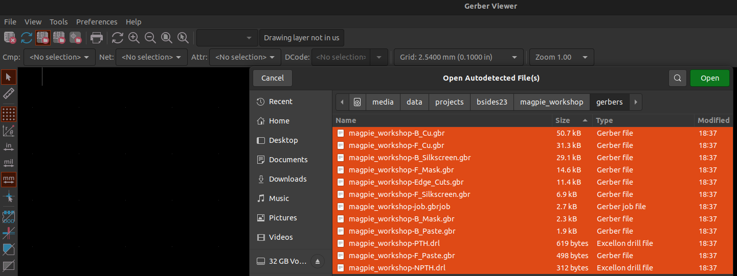
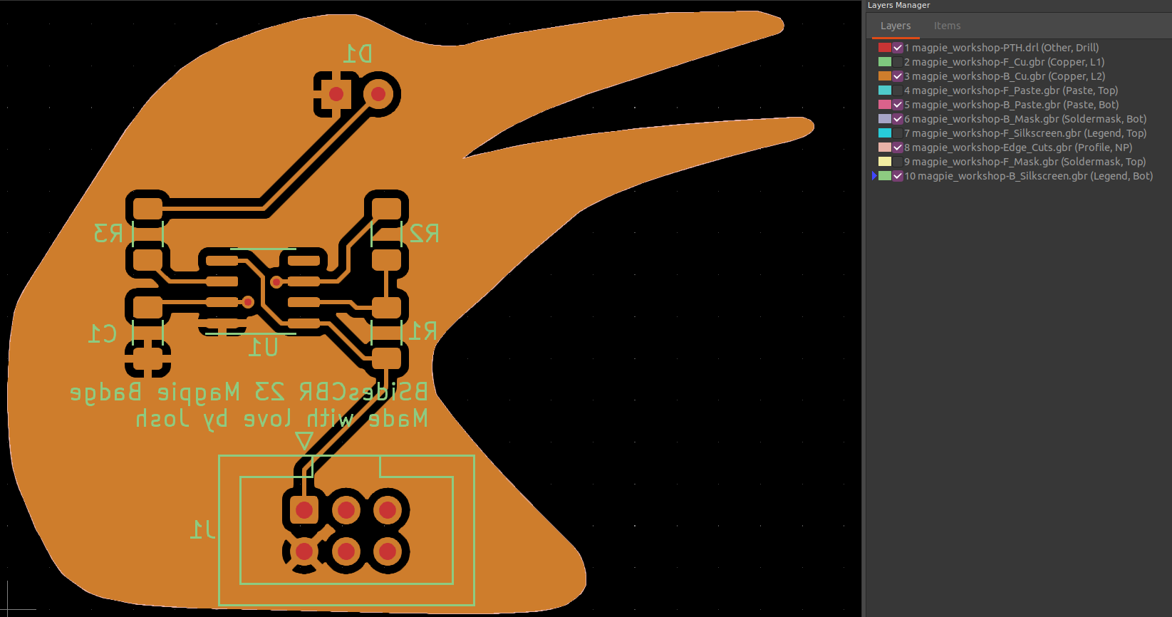
- Click on each layer to bring it to the foreground and check everything lines up / nothing looks unusual.
- Turning off layers to just look at the top / bottom of the board can help with this.
Once you are happy with the gerbers, they can be zipped up and sent off to your PCB fabricator of choice to get manufactured.
Don’t forget to order your components at this time, otherwise you won’t be able to assemble the boards once they arrive!
PCB Assembly
Once your PCBs and parts have arrived, it’s time to assemble the boards! As our board has both surface mount and through hole components, we’ll solder the surface mount components first, followed by the through hole parts.
Surface Mount Components
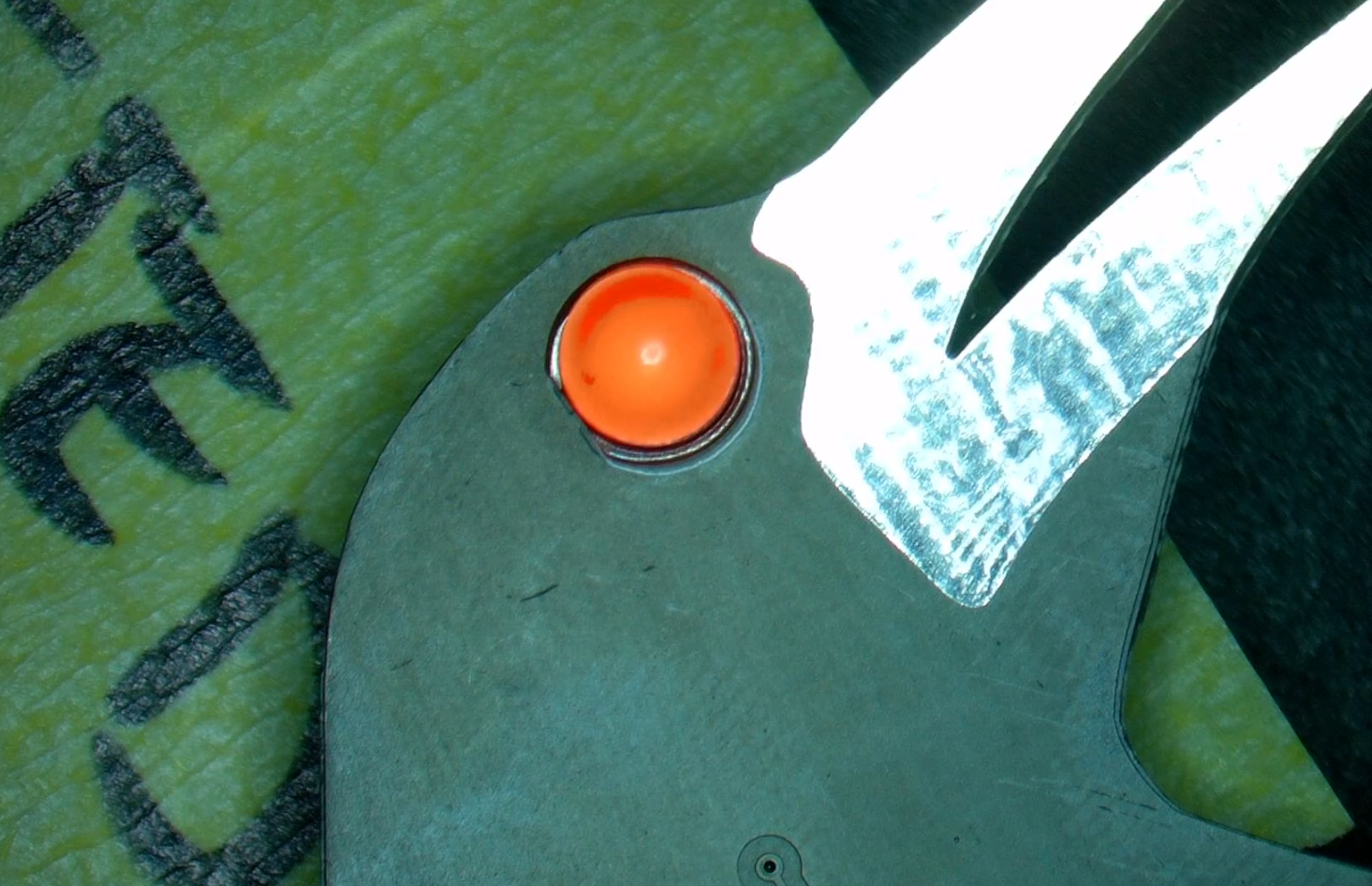
Regardless of what SMD (surface mount device) part you are soldering, the process is the same:
- Tin one pad of the PCB.
- Grab the part with your tweezers.
- Melt the solder you just put down.
- Place the part in the now molten solder and remove your iron.
- Once the part has cooled down, let go of it.
- Solder any remaining pads.
The below video shows this process.
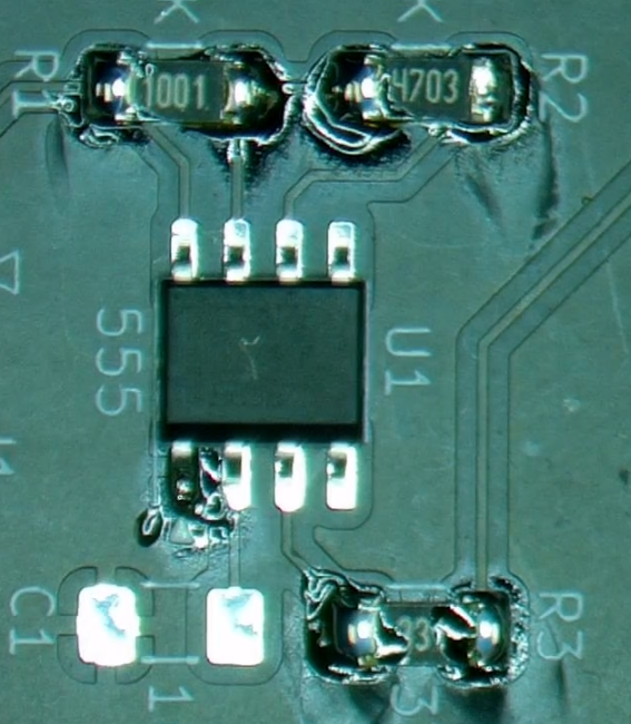
- Solder R1 (1K), R2 (470K), and R3 (330R) using the above process. Rotation / polarity does not matter.
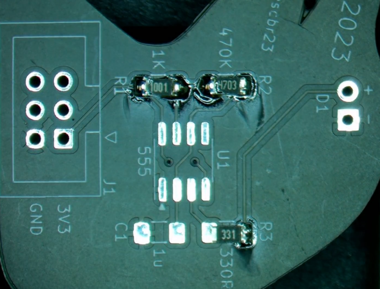
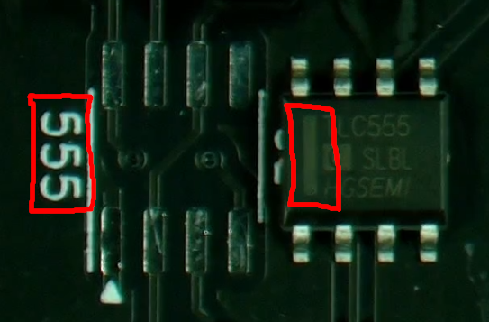
- Solder U1 (555), ensuring the bar is facing the 555 text.
- Tack one pin in place.
- Solder the remaining pins.
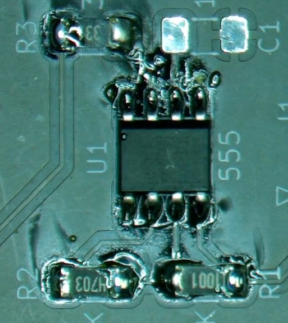
- Solder C1 (1u).
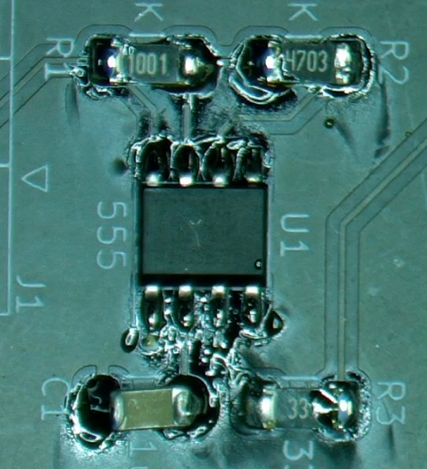
With that, all the surface mount parts are done!
Though Hole Components
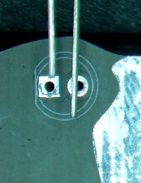
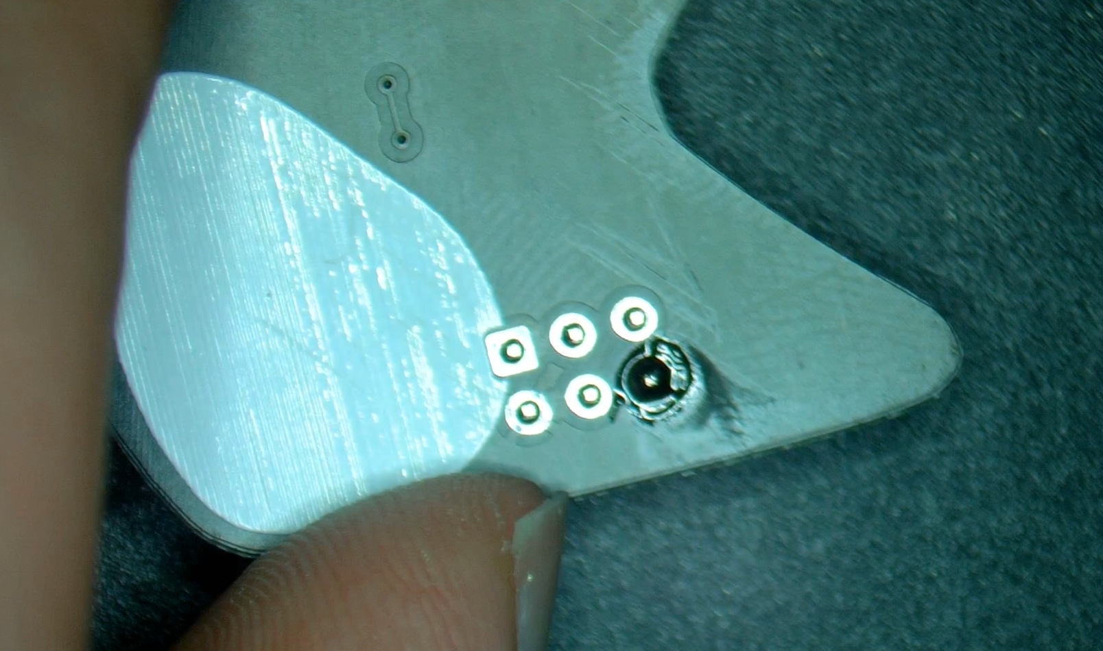
The LED is the next part to be soldered, and is polarised so rotation is important! There are two ways to orient the LED correctly:
- Line the flat side of the LED up with the flat side of the silkscreen.
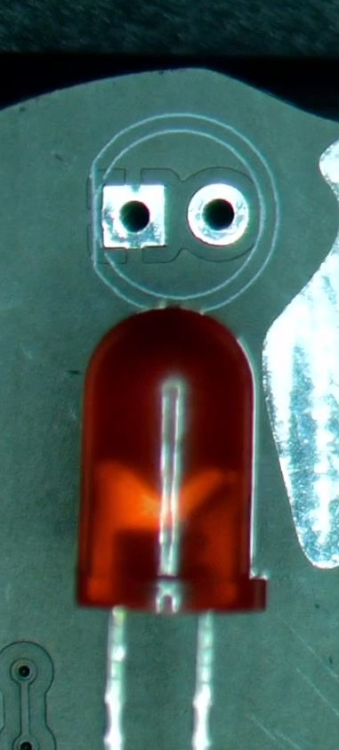
- Line the long led of the LED up with the circular hole.
- Insert the LED, flip over the PCB, and bend the LEDs so the LED stays in place. Solder the LED.
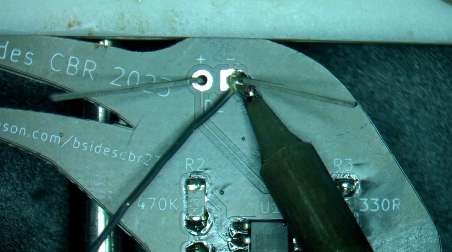
- Trim the leads, ensuring you cut towards the table as the legs will go flying!
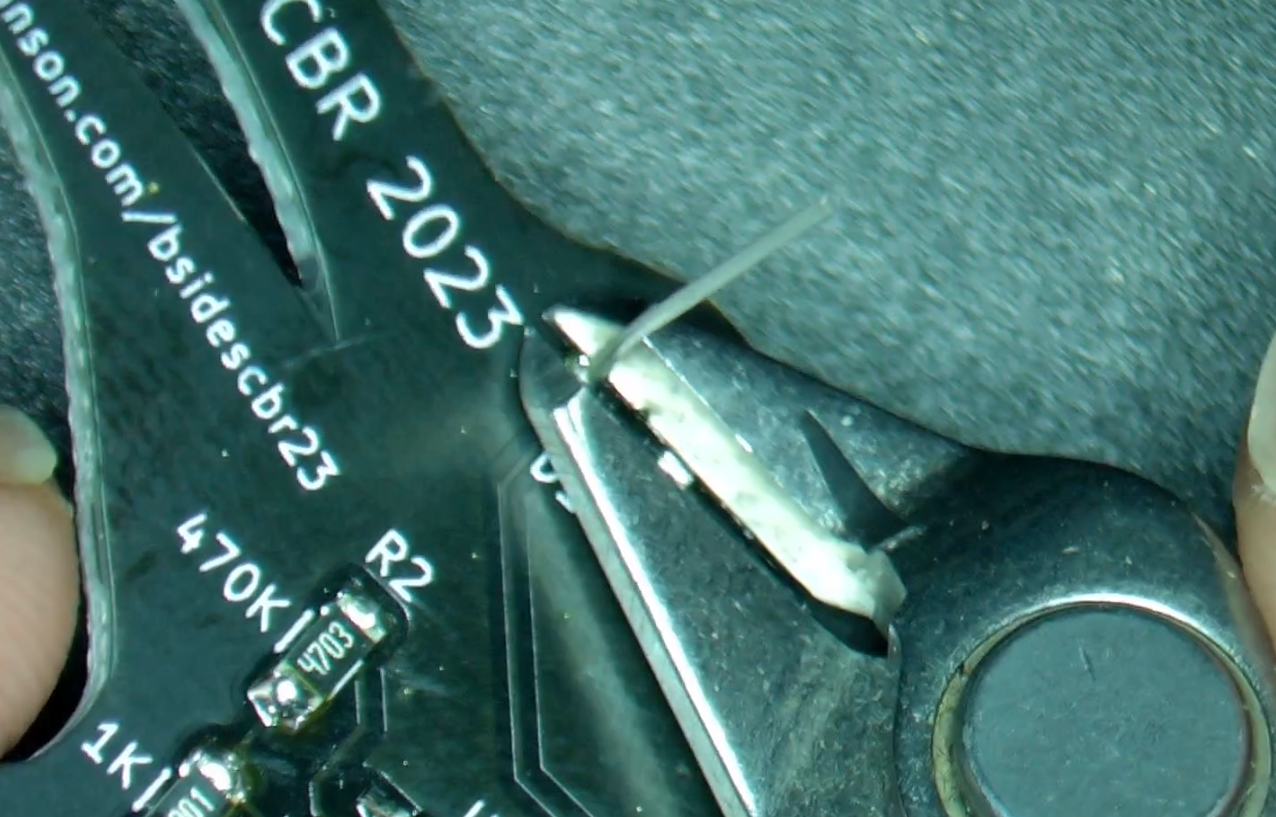
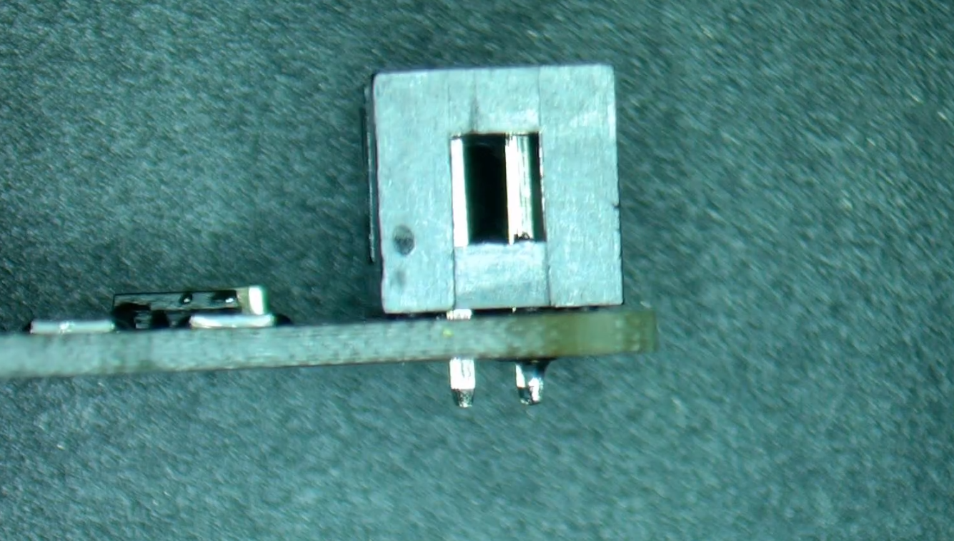
- Orient the IDC connector so the cutout is lined up with the arrow.
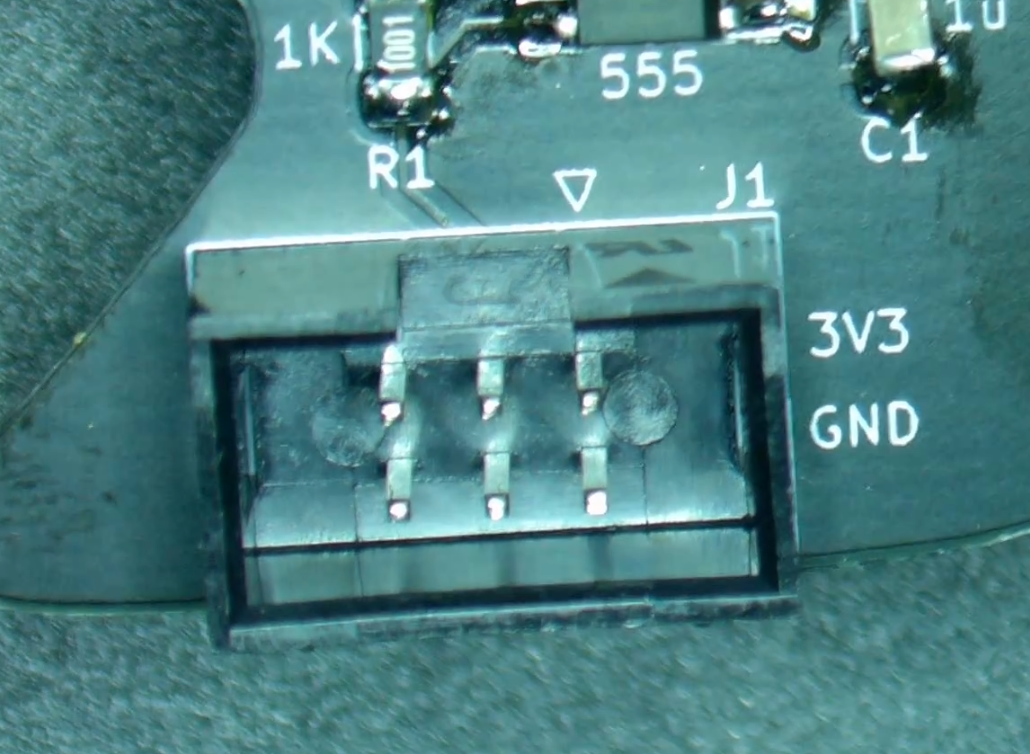
- Solder one pin of the IDC connector.
- Check the IDC connector is flush with the PCB.
Solder the remaining pins (not shown).
Finally, solder the mating connector to your badge just as you did with the IDC connector (not shown).
Smoke Test
With all the soldering done, plug the add-on into your badge and enjoy the blinking LED!
If the LED doesn’t blink, check the LED and 555 timer polarity, along with the solder joints.
Caught the soldering bug and want to buy some equipment for use at home? I have a suggested list here.
If you have any questions or feedback please let me know, otherwise thanks for attending the workshop and happy PCB designing!