
Originally posted 2019/11/18
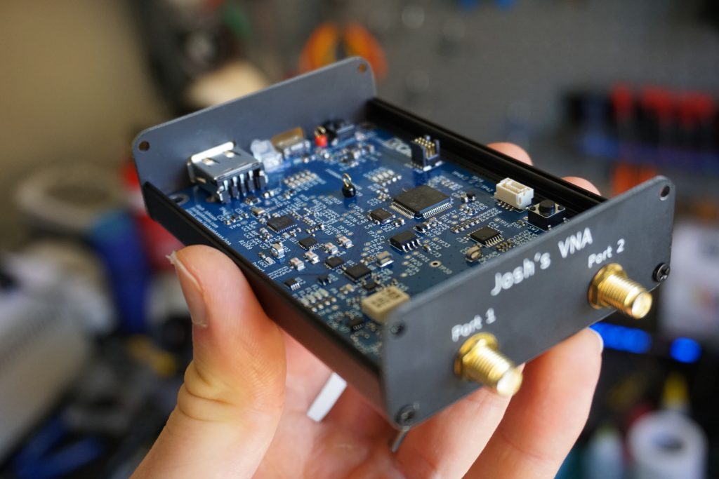
For my final year project, I set the rather ambitious goal of designing a low cost vector network analyser (VNA) which would preformant enough to deserve a spot on my bench. As you may have guessed by the title of this post, I ran into a few issues during the process which prevented the VNA from functioning well enough to be used on a day to day basis, however it was a very interesting project to work on.
For those interested the full write up of the project along with all design files can be found on github (warning 25 MB pdf), however I’ll summarise the key points from the thesis below.
Architecture
With the goal of the project to keep the price as low as possible, the design choices made at the architectural level played a key role in not only defining cost, but the function and accuracy of the device. The functional block diagram can be found below, with two key cost / performance drivers being the AD8302 gain and phase detector IC, along with the Mini Circuits ADC-15-4+ directional couplers.

The AD8302 is an RFIC which takes two RF inputs and outputs two analog voltages proportional to the phase and voltage difference between the two inputs, and enabled a low cost micro controller to be utilised to determine the magnitude and phase response of the DUT, compared to using an ADC and a bunch of DSP on a FPGA or higher end micro controller to sample, calculate, and transmit the result. This route does have decreased dynamic range, however due to the directional couplers being utilised this was not a limiting factor in the design.
One requirement I had set for the project was that all components must be COTS, as this made the design easier and cheaper to implement, with an obvious tradeoff in performance. The best directional couplers I was able to find for this project were from MiniCircuits with their ADC-15-4+, which had > 24 dB of directivity over the specified frequency range, and I was even able to push them above the 1 GHz upper frequency bound whilst maintaining enough directivity to be useful for this device.
Schematics can be found here for the VNA, along with the KiCad design files.
PCB Design
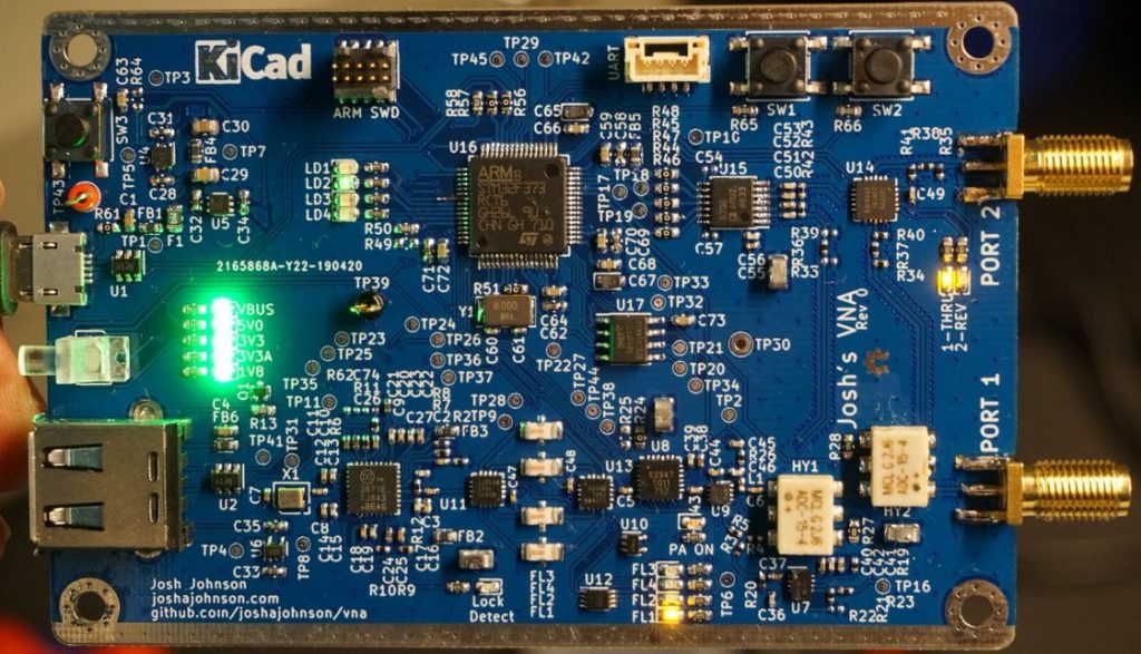
All of the above outlined components need somewhere to live, and four layers of FR4 in a signal/GND/3V3/signal configuration worked well for this application. OSHPark’s design rules were followed, as even though I would be ordering it from a Chinese board house due to my location in Australia, I wanted it to use standard processes which anyone would be able to recreate if the project was successful.
Not only was this board the most complicated board I designed / laid out to date due to the number of parts and the RF design requirements, it was also one of the earlier boards that I had used 0402 passives, QFN components, and reflowed in my modified T962 oven, and as such required a bit of rework to get it powered up without any shorts.
I was also fortunate that there only ended up being a small number of issues with the schematic / layout, with only one being critical as it was on the RF path which was easily resolved.
Firmware / Software
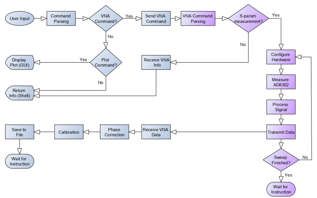
The firmware and software for the device were spit into two halves, with the STM32F373 on the VNA being responsible for low level hardware control and sending back frequency/magnitude/phase information, and Python running on a host computer to handle to user interface, do more complicated signal processing and calibration where NumPy and Scikit-rf were able to be utilised, along with proving display of the measured S parameters.
As someone whose favourite programming language is solder, I took this project as a reason to force myself to do some low level programming, with all the firmware being developed in C using ST’s HAL by yours truly. Whilst this led to many hours writing and debugging low level functions such as the USB-serial interface or the command parser, along with the struggles of bringing the MAX2871 PLL up whilst never knowing if the issue was hardware or software (note: it was both) I’m now much more comfortable with lower level firmware development which will be useful going forwards.
Performance and Function
Due to a number of issue which resulted from lack of experience on my behalf, the performance of the VNA was ultimately unsatisfactory, with the phase measurement being near useless. Whilst I won’t go into the details (thesis contains all the juicy info if you are keen) it primarily came down to a few design decisions including poor filtering of the LO’s numerous harmonics due to the divided down output, strange behaviour of the AD8302 in certain conditions, and issues during calibration caused by a difference in dynamic range between the cal standards and measured values. The first two issues could have been found and resolved with testing during the development process which was not done due to a lack of time and access to resources, and the latter may have been an easy software fix, but was found with two weeks to go and there was not enough time to resolve it.
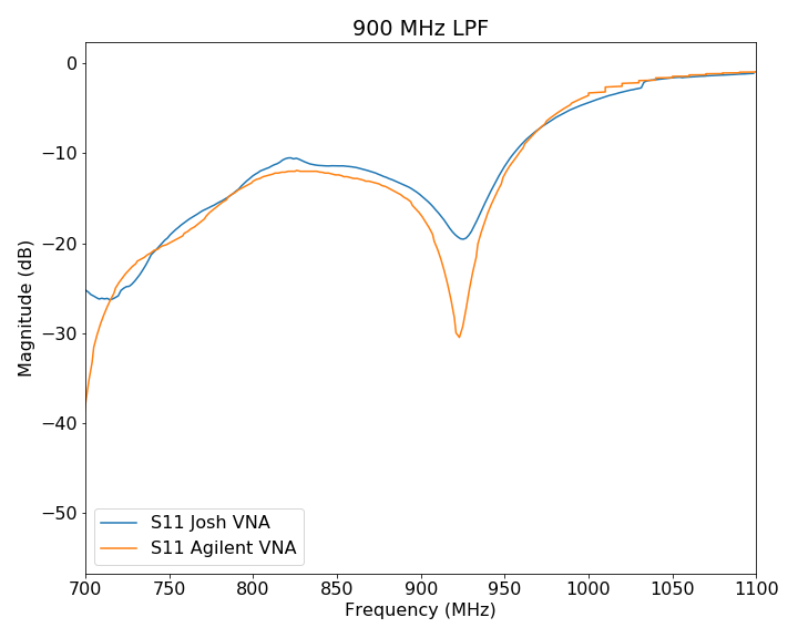
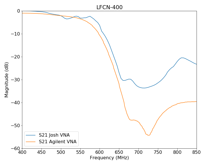
With this said, in certain situations the VNA performs well enough to be useful, as can be seen below in comparisons between my design and a commercial Agilent VNA.
Conclusion
With all of this said, the VNA is somewhat useful for measurements in the 433 and 915 MHz ISM bands if absolute accuracy is not crucial, however it won’t be replacing my desire to place a commercial VNA on by bench any time soon.
It has however provided a very useful learning experience in a bunch of areas such as RF architecture, design, and layout, firmware development, and even mechanical design, and given that I had a whole three months of RF experience before beginning this project I’m happy that it functioned at all.
What’s next? I still have few components laying around from the build so expect a small RF signal generator to make an appearance in the new year, however due to some fundamental issue with the design of the VNA I won’t be continuing it’s development any further.